
PCB Design Services
We offer robust, end-to-end PCB engineering architecture focused on standardizing industrial layouts, managing signal complexities, and delivering multi-layer board systems verified against international constraints.
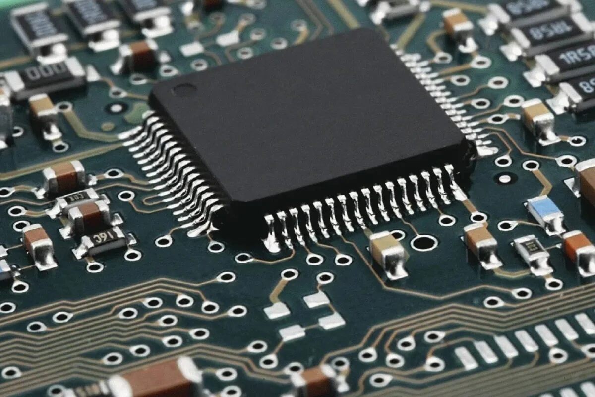
CAPABILITIES & SERVICES
Single side PCB to Multi-layer (Unlimited Layers) PCBs
HDI Designs with micro vias and advanced materials - Via-in-Pad, laser micro vias, Via stacking, Blind/Buried technology
High speed, multi-layer digital PCB designs - Bus routing, differential pairs, matched lengths.
Good knowledge in DDR2, DDR3, USB, PCIe and differential pair routing expertise High density SMT designs (BGA, uBGA, PCI, PCI Express, Mini PCI)
PCB Designs under IPC standards (Extensive RF and analog design experience (printed antennas, guard rings, RF shields...))
Designing high-speed signals by considering SI perspective and SI simulation for High-speed signals
DFX for best PCB yield from the FAB shop
Conversion between EDA tools / Reverse Engineering